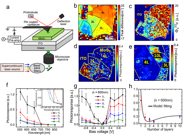
Atomically thin MoS2 is of great interest for electronic and optoelectronic applications because of its unique two-dimensional (2D) quantum confinement; however, the scaling of optoelectronic properties of MoS2 and its junctions with metals as a function of layer number as well the spatial variation of these properties remain unaddressed. In this work, we use photocurrent spectral atomic force microscopy (PCS-AFM) to image the current (in the dark) and photocurrent (under illumination) generated between a biased PtIr tip and MoS2 nanosheets with thickness ranging between n = 1 to 20 layers. Dark current measurements in both forward and reverse bias reveal characteristic diode behavior well-described by Fowler-Nordheim tunneling with a monolayer barrier energy of 0.61 eV and an effective barrier scaling linearly with layer number. Under illumination at 600 nm, the photocurrent response shows a marked decrease for layers up to n = 4 but increasing thereafter, which we describe using a model that accounts for the linear barrier increase at low n, but increased light absorption at larger n creating a minimum at n = 4. Comparative 2D Fourier analysis of physical height and photocurrent images shows high spatial frequency spatial variations in substrate/MoS2 contact that exceed the frequencies imposed by the underlying substrates. These results should aid in the design and understanding of optoelectronic devices based on quantum confined atomically thin MoS2.
http://pubs.acs.org/doi/abs/10.1021/nn506924j
The recent development of nanoelectronics using two-dimensional (2D) materials has demonstrated potential towards further miniaturization beyond Moore’s law, as well as a high-mobility solution in the emerging fields of large-area, flexible, and low-cost electronics. The 2D material that has received the most attention is graphene, a one-atom-thick, two dimensional sheet of sp2-hybridized carbon. Graphene itself is a semimetal with zero band gap, while its ultrahigh carrier mobility can provide superior current drive under low voltage bias. On the other hand, molybdenum disulfide (MoS2), a 2D semiconductor material, is attractive as a potential complement to graphene. It possesses an indirect band gap (of 1.2 eV as a multilayer and a direct band gap of 1.8 eV as a monolayer) that has enabled digital electronic components and circuits on top. Thus, a material or structure that combines the high mobility of graphene and the band gap of MoS2 would be ideal. Here, we fabricate field-effect transistor (FET) devices on the MoS2–graphene heterostructures and investigate their transport characteristics. Under negative gate bias, there exists a strong interlayer impedance due to the formation of an atomic Schottky barrier, such that the hole transport in graphene is partially, or completely, depleted. Under different drain bias, we demonstrate a new type of FET device, which enables a controllable transition from NMOS digital to bipolar characteristics. In the NMOS digital regime, we show that the on/off current ratio can be tuned to be as high as ~100, without sacrificing the field-effect mobility of graphene at room temperature. To our knowledge, this is the highest on/off current ratio ever reported in graphene-based FET devices. Accordingly, this study opens a window towards graphene-based digital and analog electronics.
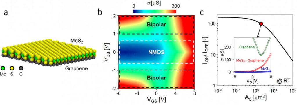
Figure 2. (a) Schematic of an MoS2-graphene heterostructure. (b) Electronic transport in an MoS2-graphene heterostructure: Measured transport characteristics for a trilayer MoS2-graphene FET device (AC ~ 12 mm2) as a function of VGS and VDS at room temperature. (c) Engineering on/off current ratio in the MoS2-graphene FET device considered by tuning the contact area AC: Calculated Ion/Ioff at room temperature and VDS = 10 mV as a function of AC. The inset corresponds to the calculated transport curve for AC = 1 mm2 (red). The measured transport curves for our representative MoS2 (blue) and Graphene (green) FET devices are also shown for comparison.
Link:
Shih, C.-J., Wang, Q. H., Son, Y., Jin, Z., Blankschtein, D., Strano, M. S. Tuning on–Off Current Ratio and Field-Effect Mobility in a MoS2–Graphene Heterostructure Via Schottky Barrier Modulation. ACS Nano 2014, 8, 5790-5798